- 您现在的位置:买卖IC网 > Sheet目录3872 > PIC18F4450T-I/ML (Microchip Technology)IC PIC MCU FLASH 8KX16 44QFN
212
XMEGA A [MANUAL]
8077I–AVR–11/2012
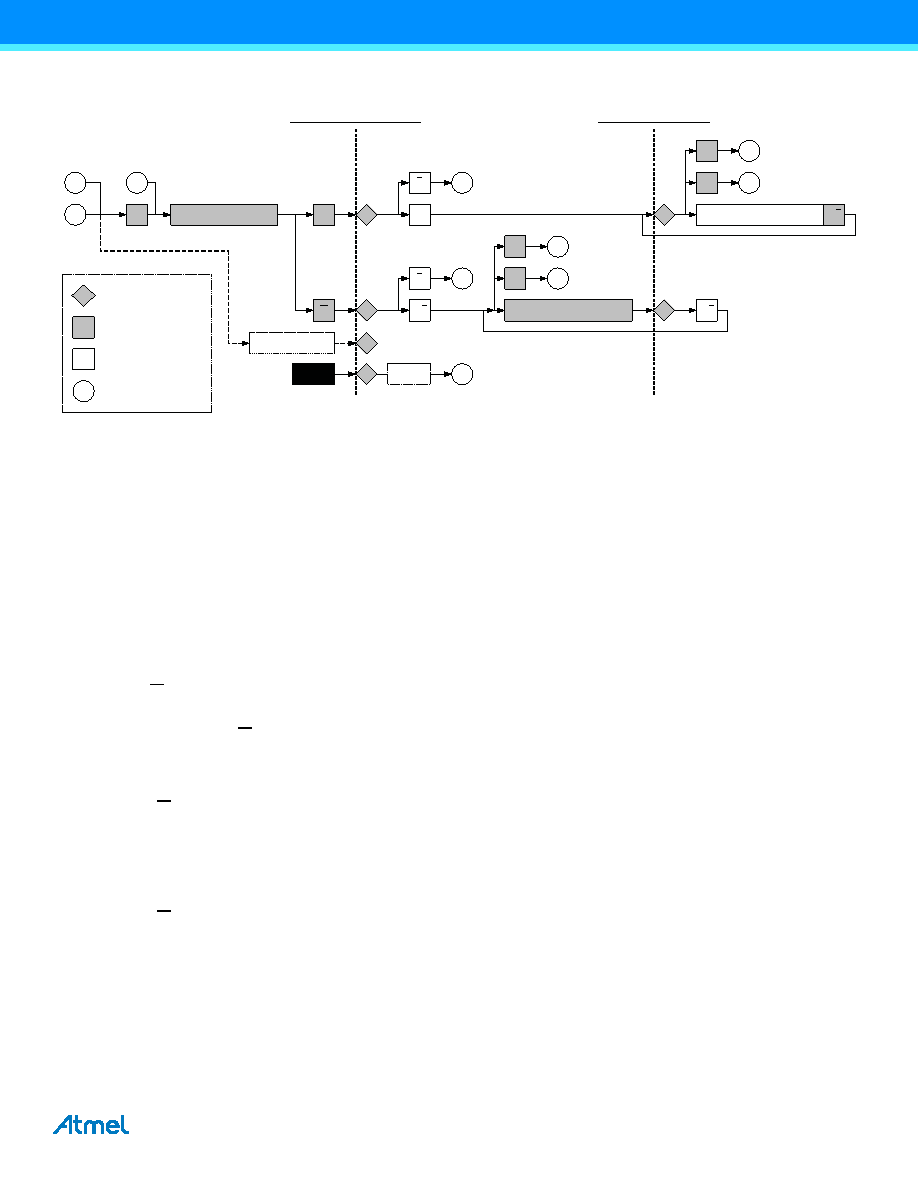
Figure 19-13.TWI slave operation.
The number of interrupts generated is kept to a minimum by automatic handling of most conditions. Quick command can
be enabled to auto-trigger operations and reduce software complexity.
Promiscuous mode can be enabled to allow the slave to respond to all received addresses.
19.6.1 Receiving Address Packets
When the TWI slave is properly configured, it will wait for a START condition to be detected. When this happens, the
successive address byte will be received and checked by the address match logic, and the slave will ACK a correct
address and store the address in the DATA register. If the received address is not a match, the slave will not
acknowledge and store address, and will wait for a new START condition.
The slave address/stop interrupt flag is set when a START condition succeeded by a valid address byte is detected. A
general call address will also set the interrupt flag.
A START condition immediately followed by a STOP condition is an illegal operation, and the bus error flag is set.
The R/W direction flag reflects the direction bit received with the address. This can be read by software to determine the
type of operation currently in progress.
Depending on the R/W direction bit and bus condition, one of four distinct cases (S1 to S4) arises following the address
packet. The different cases must be handled in software.
19.6.1.1 Case S1: Address packet accepted - Direction bit set
If the R/W direction flag is set, this indicates a master read operation. The SCL line is forced low by the slave, stretching
the bus clock. If ACK is sent by the slave, the slave hardware will set the data interrupt flag indicating data is needed for
transmit. Data, repeated START, or STOP can be received after this. If NACK is sent by the slave, the slave will wait for
a new START condition and address match.
19.6.1.2 Case S2: Address packet accepted - Direction bit cleared
If the R/W direction flag is cleared, this indicates a master write operation. The SCL line is forced low, stretching the bus
clock. If ACK is sent by the slave, the slave will wait for data to be received. Data, repeated START, or STOP can be
received after this. If NACK is sent, the slave will wait for a new START condition and address match.
19.6.1.3 Case S3: Collision
If the slave is not able to send a high level or NACK, the collision flag is set, and it will disable the data and acknowledge
output from the slave logic. The clock hold is released. A START or repeated START condition will be accepted.
S
S3
ADDRESS
S2
A
S1
R
W
DATA
A/A
DATA
P
S2
Sr
S3
P
S2
Sr
S3
SLAVE ADDRESS INTERRUPT
SLAVE DATA INTERRUPT
A
Collision
(SMBus)
SW
A/A
SW
Release
Hold
S1
A
S1
SW
Interrupt on STOP
Condition Enabled
S1
SW
Driver software
The master provides data
on the bus
Slave provides data on
the bus
Sn
Diagram connections
发布紧急采购,3分钟左右您将得到回复。
相关PDF资料
PIC18F4321T-I/ML
IC PIC MCU FLASH 4KX16 44QFN
PIC18F4221T-I/ML
IC PIC MCU FLASH 2KX16 44QFN
PIC18F2321T-I/ML
IC PIC MCU FLASH 4KX16 28QFN
PIC18F2221T-I/SO
IC PIC MCU FLASH 2KX16 28SOIC
PIC16LF1939-I/MV
IC MCU 8BIT 28KB FLASH 40-UQFN
PIC24F16KL402-I/SP
IC MCU 16BIT 16KB FLASH 28-SPDIP
PIC18F24J11-I/SS
IC PIC MCU FLASH 16K 2V 28-SSOP
PIC24F16KA101-I/SO
IC PIC MCU FLASH 16K 20-SOIC
相关代理商/技术参数
PIC18F4450T-I/PT
功能描述:8位微控制器 -MCU 16KB FL 768 RAM 34 I/O FS-USB 2.0 RoHS:否 制造商:Silicon Labs 核心:8051 处理器系列:C8051F39x 数据总线宽度:8 bit 最大时钟频率:50 MHz 程序存储器大小:16 KB 数据 RAM 大小:1 KB 片上 ADC:Yes 工作电源电压:1.8 V to 3.6 V 工作温度范围:- 40 C to + 105 C 封装 / 箱体:QFN-20 安装风格:SMD/SMT
PIC18F4455-BL
制造商:POWERLITE SYSTEMS 功能描述:PIC18F445 W/ BOOTLOADER FOR FLASHLAB 制造商:POWERLITE SYSTEMS 功能描述:PIC18F445 W/ BOOTLOADER, FOR FLASHLAB 制造商:POWERLITE SYSTEMS 功能描述:PIC18F445 W/ BOOTLOADER, FOR FLASHLAB; Silicon Manufacturer:Powerlite Systems; Core Architecture:PIC; Kit Contents:Board; Features:Bootloader Programming, RS232 Connector for Boot-Loading and Serial Comms ;RoHS Compliant: Yes
PIC18F4455-I/ML
功能描述:8位微控制器 -MCU 24kBF 2048RM FSUSB2 RoHS:否 制造商:Silicon Labs 核心:8051 处理器系列:C8051F39x 数据总线宽度:8 bit 最大时钟频率:50 MHz 程序存储器大小:16 KB 数据 RAM 大小:1 KB 片上 ADC:Yes 工作电源电压:1.8 V to 3.6 V 工作温度范围:- 40 C to + 105 C 封装 / 箱体:QFN-20 安装风格:SMD/SMT
PIC18F4455-I/P
功能描述:8位微控制器 -MCU 24kBF 2048RM FSUSB2 RoHS:否 制造商:Silicon Labs 核心:8051 处理器系列:C8051F39x 数据总线宽度:8 bit 最大时钟频率:50 MHz 程序存储器大小:16 KB 数据 RAM 大小:1 KB 片上 ADC:Yes 工作电源电压:1.8 V to 3.6 V 工作温度范围:- 40 C to + 105 C 封装 / 箱体:QFN-20 安装风格:SMD/SMT
PIC18F4455-I/PT
功能描述:8位微控制器 -MCU 24kBF 2048RM FSUSB2 RoHS:否 制造商:Silicon Labs 核心:8051 处理器系列:C8051F39x 数据总线宽度:8 bit 最大时钟频率:50 MHz 程序存储器大小:16 KB 数据 RAM 大小:1 KB 片上 ADC:Yes 工作电源电压:1.8 V to 3.6 V 工作温度范围:- 40 C to + 105 C 封装 / 箱体:QFN-20 安装风格:SMD/SMT
PIC18F4455T-I/ML
功能描述:8位微控制器 -MCU 24kBF 2048RM FSUSB2 RoHS:否 制造商:Silicon Labs 核心:8051 处理器系列:C8051F39x 数据总线宽度:8 bit 最大时钟频率:50 MHz 程序存储器大小:16 KB 数据 RAM 大小:1 KB 片上 ADC:Yes 工作电源电压:1.8 V to 3.6 V 工作温度范围:- 40 C to + 105 C 封装 / 箱体:QFN-20 安装风格:SMD/SMT
PIC18F4455T-I/PT
功能描述:8位微控制器 -MCU 24kBF 2048RM FSUSB2 RoHS:否 制造商:Silicon Labs 核心:8051 处理器系列:C8051F39x 数据总线宽度:8 bit 最大时钟频率:50 MHz 程序存储器大小:16 KB 数据 RAM 大小:1 KB 片上 ADC:Yes 工作电源电压:1.8 V to 3.6 V 工作温度范围:- 40 C to + 105 C 封装 / 箱体:QFN-20 安装风格:SMD/SMT
PIC18F4458-I/ML
功能描述:8位微控制器 -MCU 24KB Flash 2KB RAM RoHS:否 制造商:Silicon Labs 核心:8051 处理器系列:C8051F39x 数据总线宽度:8 bit 最大时钟频率:50 MHz 程序存储器大小:16 KB 数据 RAM 大小:1 KB 片上 ADC:Yes 工作电源电压:1.8 V to 3.6 V 工作温度范围:- 40 C to + 105 C 封装 / 箱体:QFN-20 安装风格:SMD/SMT